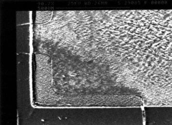
Description:
Hardly detectable rupture of conductor at the end of the solder joint of a component. Excessive mechanical stress caused this rupture. It is primarily the thickness of the copper foil which influences the frequency of this defect which only occurs, however, if the PCB is bent considerably ( separation of the web). In most of the cases the (ceramic) components already fail earlier due to mechanical destruction.
Causes/Remedy:
- inexpert mechanical handling of assembly
- different coefficients of expansion of materials to be joined
 Source:
SEM
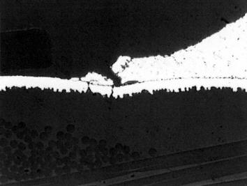
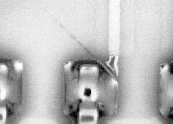
Description:
This is a micrograph of the soldering defect shown before. The ruptured conductor is clearly visible.
Causes/Remedy:
- inexpert mechanical handling of assembly
- different coefficients of expansion of materials to be joined
 Source:
Microsection
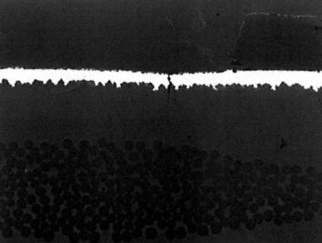
Description:
Ruptured conductor. Apart from excessive mechanical stress (bending, torsion), temperature changes can also damage conductors, because the varying expansion of copper and base material respectively cause mechanical stress.
Causes/Remedy:
- inexpert mechanical handling of assembly
- different coefficients of expansion of materials to be joined
 Source:
Microsection
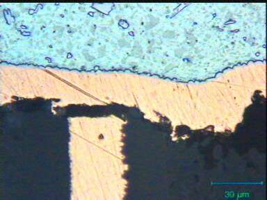
Description:
Ruptured conductor on an internal layer in a multilayer PCB. This defect is not visible from outside, so that there is no repair possibility, and it can only be proven by means of a destructive microsection. It is true that the defect can be located through electrical measuring, but this is very cost intensive. These defects are caused by mechanical stress (minor percentage) and faulty manufacture of the multilayer board (major percentage).
Causes/Remedy:
- extensive mechanical stress
- manufacturing faults
- different coefficients of expansion of materials to be joined
 Source:
Microsection
Description:
Mechanically caused rupture of a conductive path on a ceramic carrier (hybrid). Inexpert handling (e.g. with a tool) caused this conductor to crack. In this case the hybrid should be replaced and not the defect repaired (for reasons of reliability).
Causes/Remedy:
- inexpert mechanical handling of assembly
- unsuited or wrongly used tools
 Source:
visual, optical inspection - general view
Our analytics team can help you find the cause.
go to failure analysis at TechnoLab