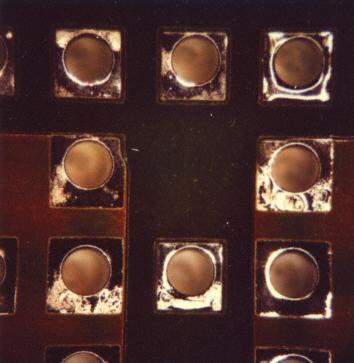
Bad tinning
Description:
Bad tinning of some parts of conductors. The copper areas partly visible (reddish) reveal a bad wettability of the copper. This can be caused by contaminated or corroded copper areas, in fery few cases by the hot tinning process itself.
Causes/Remedy:
- contamination of copper areas
- corrosion of copper areas
- deficiencies in the tinning process (temperature, alloy)
 Source:
visual, optical inspection - general view
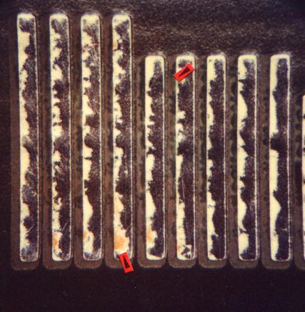
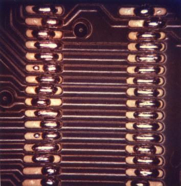
Inhomogenous tinning
Description:
Inhomogenous tinning. Excess solder in certain areas is characteristic of this. The distribution and thus the thickness of the layer is inhomogenous, (frequent phenomenon with hot air tinning). This defect is acceptable, as long as all areas are wetted with solder.
Causes/Remedy:
- deficiencies in the tinning process
- impaired local wettability of copper areas, in most of the cases due to contamination
 Source:
visual, optical inspection - general view
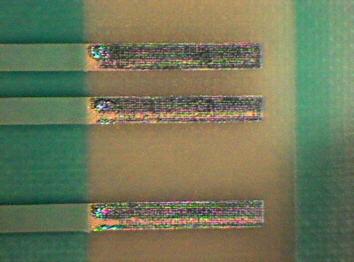
Disturbed tinning
Description:
Disturbed tinning on pads (bluish areas). Rough surface after tinning hinting to contamination of solder alloy and partially unwettable areas on pads.
Causes/Remedy:
- deficiencies in the tinning process
- impaired local wettability of copper areas, in most of the cases due to contamination
- corrosions
 Source:
visual, optical inspection - general view
Strongly impaired wetting
Description:
Strongly impaired wetting of tinning at parts of conductors. The area shining reddish marks the copper areas which have not been wetted. Rework necessary.
Causes/Remedy:
- deficiencies in the tinning process
- impaired local wettability of copper areas, in most of the cases due to contamination
- Corrosions
 Source:
visual, optical inspection - general view
Whisker
Description:
Whisker in plated through-hole (thin single crystal, grown in the wall, needle-shaped). Unsuited combinations of different materials lead to material stress which can cause the growing of single crystals on the surface.
Causes/Remedy:
- Addition of elements to alloy (lead, bismuth)
- integrate intermetallic zone (Ni interlayer)
 Source:
visual, optical inspection - general view
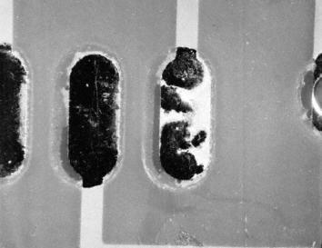
Failed tinning
Description:
Failed tinning on pads of circuit. Due to very bad wetting of the pads the solder contracted and did not form a flat wetted surface. Not acceptable.
Causes/Remedy:
- hardly wettable pads
- contamination
- contaminated solder alloy for tinning
 Source:
visual, optical inspection - general view
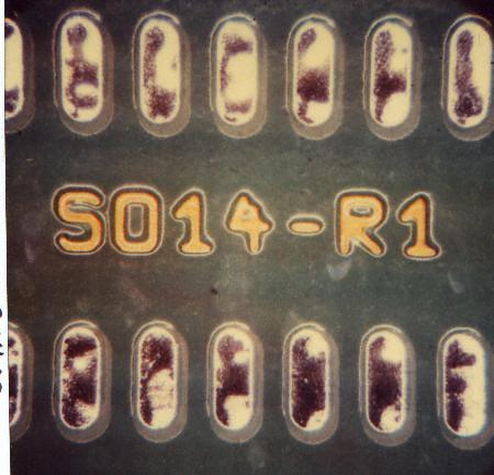
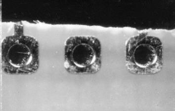
Inhomogenous layer thickness
Description:
Inhomogenous layer thickness of tinning at eyelets. Bad wetting of copper areas or deficiencies in the hot tinning process can cause this defect.
Causes/Remedy:
- tinning deficiencies
- impaired local wettability of copper areas, in most of the cases due to contamination
 Source:
visual, optical inspection - general view
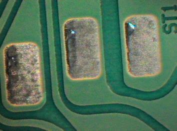
Tinning deficiencies
Description:
Tinning deficiencies at pads due to corrosion on pads (dark areas). Not acceptable.
Causes/Remedy:
- tinning deficiencies
- impaired local wettability of copper areas, in most of the cases due to contamination
- corrosion of pads
 Source:
visual, optical inspection - general view
Our analytics team can help you find the cause.
go to failure analysis at TechnoLab