Passive SMD components: Lifting-off of one end of the component from the joining surface, reaching from just-not-connected-any-more (crocodile's snout) to the vertical position (tombstone or drawbridge or Manhattan effect)
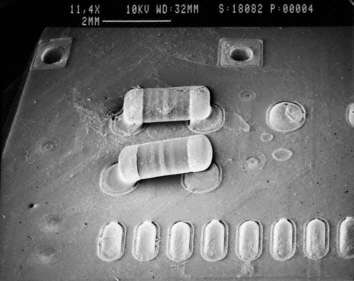
Tombstoning of CMC
Description:
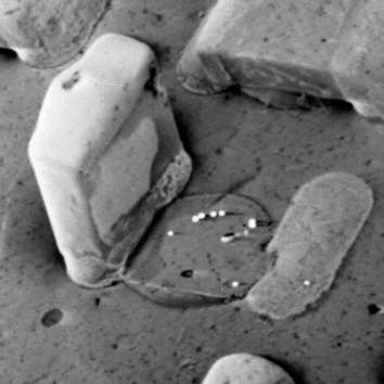
Tombstoning of a CMC 1812. The example shown on the left is no real tombstone effect although the appearance is typical of it. In this case the component has come off its adhesive fixing and was lifted up during the wave soldering process (see residue of adhesive on PCB). When the temperature sank below the liquidus, the component was then vertically soldered on a landing pad. This component has to be replaced during rework. soldering tip temperature ≤ 360°C (sensitive ceramic component)
Causes/Remedy:
- insufficient hardening of adhesive
- poor wetting (right), since residues of adhesive on pad
- unsuitable soldering parameter
- vibration of assembly during transport within soldering system
 Source:
SEM
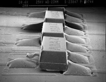
Tombstoning of MiniMELF
Description:
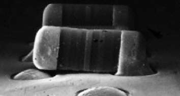
Tombstoning of a MiniMELF. It can be clearly seen that the component is tilted. In this case the solder joint on the right side melted first and then , through its surface tension, drew up the component. The component is tilted and could therefore not be soldered on the left side. It has to be completely replaced during rework.
Causes/Remedy:
- poor heat distribution during reflow soldering
- inhomogenous heat energy distribution due to conductors of different widths
- inhomogenous solder paste printing
 Source:
SEM
Description:
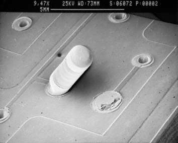
Typical tombstoning of a MiniMELF in the reflow process. Clearly visible lifting-off of the component. Extreme example
Causes/Remedy:
- poor heat distribution during the reflow process
- inhomogenous flow of heat energy, due to conductors of different widths
- inhomogenous solder paste printing
 Source:
SEM
Description:
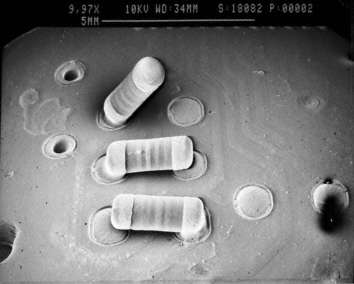
Tombstoning at different stages. The wettability of the components influences this effect to a considerble extent.
Causes/Remedy:
- poor heat distribution during the reflow process
- inhomogenous flow of heat energy, due to conductors of different widths
- inhomogenous solder paste printing
 Source:
SEM
Description:
Further example of tombstoning of a MiniMELF (bottom).
Causes/Remedy:
- poor heat distribution during the reflow process
- inhomogenous flow of heat energy, due to conductors of different widths
- inhomogenous solder paste printing
 Source:
SEM
Tombstoning of SOT23
Description:
Tombstoning of a SOT23. In this case the combination of inhomogenous heat distribution and a component lead slightly bent upwards (left) was responsible for the non-soldering. During rework the component should be completely removed and refitted according to the standard.
Observe ESD protection measures !
Causes/Remedy:
- poor hear distribution during reflow soldering
- inhomogenous heat energy distribution due to conductors of different widths
- compoent lead bent
 Source:
SEM
Tombstoning of SOD
Description:
Tombstoning of a SOD. The example shown on the left is no real tombstone effect although the appearance is typical of it. In this case the component has come off its adhesive fixing and was lifted up during the wave soldering process (see residue of adhesive on PCB). When the temperature sank below the liquidus, the component was vertically soldered on a landing pad. This component has to be replaced during rework. soldering tip temperature ≤ 360°C
Causes/Remedy:
- insufficient curing of adhesive
- poor wetting (right), since residues of adhesive on pad
- unsuitable soldering parameter
- vibration of assembly during transport within soldering system
 Source:
visual, optical inspection - general view
Our analytics team can help you find the cause.
go to failure analysis at TechnoLab