Missing solder fillet, insufficient or altogether missing wetting of one or both of the surfaces to be joined, no (mechanical) connection.
Opens at BGA
Description:
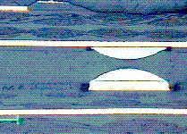
Open at a BGA. For constructional reasons this defect cannot be seen from outside . It is therefore difficult to locate. The microsection and previous X-ray inspection, however, clearly reveal this defect.
Causes/Remedy:
- BGA/PCB not coplanar
- vibration during transport
- insufficient solder paste application
- deformation of BGA/PCB during soldering
 Source:
Microsection
Description:
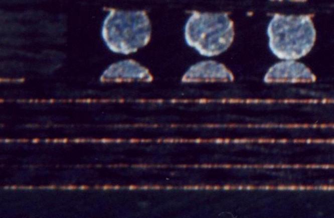
Opens at a BGA. In this example many joints were not soldered due to the component lifting off on one side or due to thermal deformation.
Causes/Remedy:
- Monitor transport of components before and during the soldering process
- Bear in mind popcorning effect of large plastic casings!
 Source:
Microsection
Description:
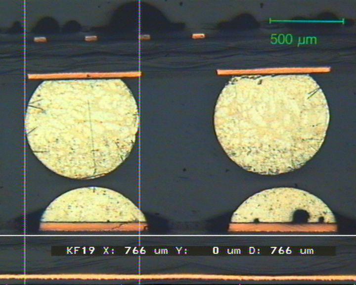
Opens at a BGA. The gap between the solder depots to be joined is clearly visible. This defect is due to movements or lifting-off of the component. Attention: Such defects cannot always be detected with X-ray inspection systems.
Causes/Remedy:
- Monitor transport of components before and during the soldering process
- Bear in mind popcorning effect of large plastic casings !
 Source:
Microsection
Opens at CMC
Description:
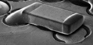
Open at a CMC during wave soldering. The defect is clearly visible from outside. Rework/Repair is easily done but has to match the sensible components. Soldering tip temperature ≤ 360°C.
Causes/Remedy:
-
Shadow effect during soldering, therefore:
- poor layout
- locally disturbed flux application
- bad wettability of component
- residue of adhesive on pad
 Source:
SEM
Description:
Clearly visible open at a CMC after wave soldering. The solder joints are easily accessible; therefore the defect can be quickly located.
Causes/Remedy:
- shadow effect during soldering
- unwettable components
- partially contaminated landing pads
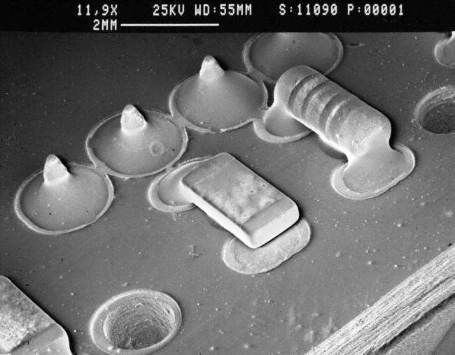 Source:
SEM
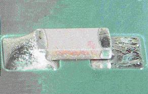 Source:
visual, optical inspection - general view
Opens at DIP
Description:
Open at a DIP component. A poor solder fillet (left) or missing wetting (right) prevent solder joints. The contact is only loosely connected but not soldered. Visually distinct defect. Rework has to make sure that the solder completely fills the through-hole. Pay attention to solder contact time and soldering temperature (≤ 360°C).
Observe precautions for handling ESD!
Causes/Remedy:
- wetting deficiencies at leads
- solder contact time during wave soldering too short
- damaged through-hole
- soldering temperature insufficient
- flux does not reach relevant area
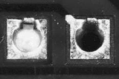 Source:
visual, optical inspection - general view
Description:
Open at two DIP leads for THT. It is clearly visible where solder is lacking at the holes and around the leads.
Causes/Remedy:
- poor wettability of leads
- residues/contamination in the holes
- poor metallic structure in the holes (tinning)
- unsuited layout for the wave soldering direction
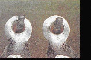 Source:
visual, optical inspection - general view
Description:
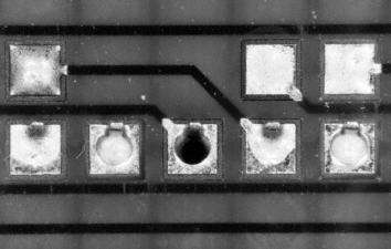
Open and poor solder fillets at a DIP. Same context as described above.
Causes/Remedy:
- poor wettability of leads
- residues/contamination in the holes
- poor metallic structure in the holes (tinning)
- unsuited layout for the wave soldering direction
 Source:
visual, optical inspection - general view
Opens at DPAK
Description:
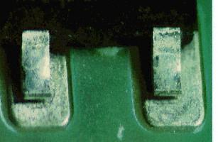
Open at a DPAK component. In this case missing solder paste caused the defect. As the component was soldered on one side (not visible on photo) the leads have slightly lifted off on the other. This facilitates visual inspection, since there is a distinct gap between pad and lead ( also see other examples). It is recommended to remove the component completely and to resolder it by hand. Pay attention to soldering temperature (≤ 360°C).
Observe precautions for handling ESD!
Causes/Remedy:
- faulty solder paste application In case solder paste has been applied correctly:vv
- bear in mind possible tombstone effect
- wetting deficiencies at leads through contact material (Alloy 42)
 Source:
visual, optical inspection - general view
Description:
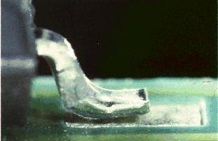
Open at the lead of a DPAK. The reflow soldering process could not produce a solder joint since the solder paste was missing. Moreover the lead does not lie flat on the pad. (coplanarity problem)
Causes/Remedy:
- poor solder paste application
 Source:
visual, optical inspection - general view
Opens at MiniMELF
Description:
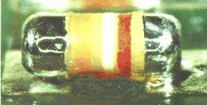
Open at a MiniMELF resistor during reflow soldering. The defect is easily detectable from outside. Rework has to match the component. Soldering tip temperature ≤ 360 °C.
Causes/Remedy:
- too little solder paste applied
- solder paste missing
- wetting deficiencies of component
 Source:
visual, optical inspection - general view
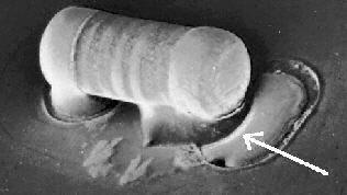
Description:
Open at a resistor in MiniMelf shape. Since the adhesive was not applied in the correct position the wave soldering process could not produce a solder joint (adhesive is on the contact pad). The component should be removed completely and a new one mounted. Excess adhesive is to be removed as well.
Causes/Remedy:
- positioning fault in adhesive application
- smearing of adhesive because of manual contact
- unsuitable properties of adhesive (temperature, viscosity)
 Source:
SEM
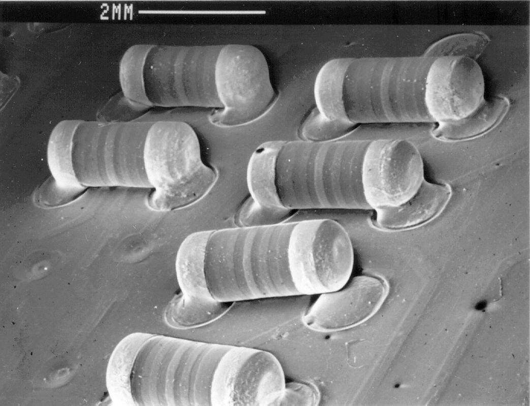
Description:
Open at a MiniMelf component after reflow soldering. The contact area (right) of the component is simply lying on the unmolten solder depot without forming an electrical and mechanical contact. This can already be classified as a tombstone effect. Simple rework through renewed soldering.
Causes/Remedy:
- uneven application of solder paste (quantity)
- inhomogeneous heat distribution
- layout faults (heat flow)
 Source:
SEM
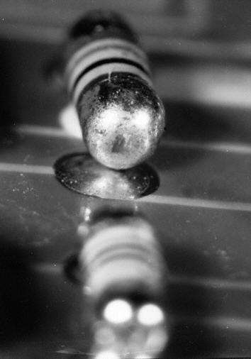
Description:
Open at a MiniMelf resistor after wave soldering. It can be clearly seen where the solder fillet is missing between the component and contact pad. Rework through renewed soldering is easy. Observe soldering tip temperature.
Causes/Remedy:
- Shadowing effect during wave soldering
- poor wettability of components
- contamination of landing pads and/or components
 Source:
visual, optical inspection - general view
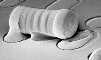
Description:
Open at a resistor after wave soldering. Non-qualified residues on the right landing pad prevented soldering This shows the effect which even the slightest contamination has on the formation of acceptable soldering joints. Rework is necessary, and it should also be analysed how the contamination was possible.
Causes/Remedy:
- residues on the landing pads impairing wettability
- contact pads partly missing metal
- residues from adhesive application (Fädenbildung)
 Source:
SEM
Opens at PLCC
Description:
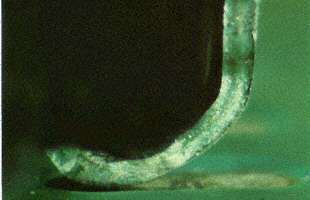
Open at a PLCC (J-lead). This defect cannot always be easily detected from outside, especially if it is rather located in the middle. Rework, however, is unproblematic. Make sure that repair does not result in excess solder.
Observe precautions for handling ESD!
Causes/Remedy:
- solder paste missing
- too little solder paste applied
- bad wettability of leads (especially with Alloy42)
- bent, deformed leads
 Source:
visual, optical inspection - general view
Opens at QFP
Description:
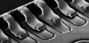
Open at several leads of a QFP. This defect is easily detectable in general, since the leads are visible from outside. Rework has to make sure not to use excess solder.
Observe precautions for handling ESD!
Causes/Remedy:
- solder paste missing
- too little solder paste applied
- component not coplanar
- wetting deficiencies at leads
- bent, deformed leads
 Source:
SEM
Description:
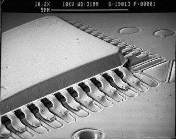
Opens at a QFP. This is the example shown in the main file but a general view of it. The high number of unsoldered leads at the bottom is clearly visible.
Causes/Remedy:
- solder paste missing
- insufficient solder paste application
- coplanarity problems of the component
- poor wetting of the leads
- leads bent, deformed
 Source:
SEM
Opens at SO
Description:
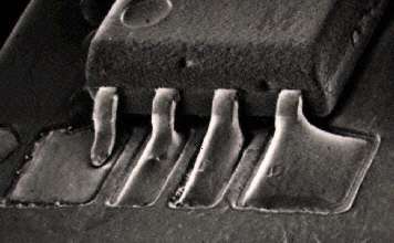
Open at a SO8. The pads at the corners which are larger than the others are to act as solder thieves during wave soldering. The defect is clearly visible. Rework has to make sure that solder joints are uniform.
Observe precautions for handling ESD!
Causes/Remedy:
- wetting deficiencies of leads
- shadow effect during wave soldering
- poorly dimensioned pads
- wetting deficiencies at PCB
 Source:
SEM
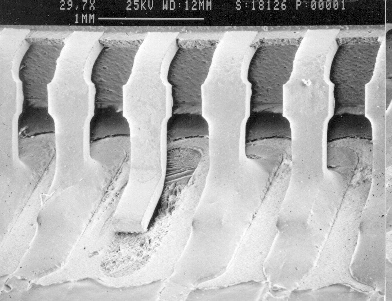
Description:
Open at a SO-IC. In this case the solder joint was not formed because of missing solder paste. This defect can easily be distinguished from the normal solder joints.
Causes/Remedy:
- contamination on the landing pad
- landing pad oxidized
- solder paste missing
 Source:
SEM
Opens at SOT23
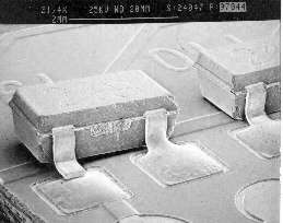
Description:
Open at a SOT23 during the reflow process. Visual inspection easily locates this defect. It can be seen that one of the contacts has lifted off so that it could not be wetted any more. Rework has to make sure to achieve geometrically uniform solder joints.
Observe precautions for handling ESD!
Causes/Remedy:
- bent, deformed leads
- deficiencies in the placing process
- melting during reflow not simultaneous
- beginning tombstone effect
- wetting deficiencies at leads
 Source:
SEM
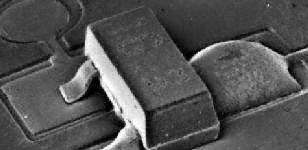
Description:
Open (left) at a SOT23 after wave soldering.
Causes/Remedy:
- poor wettability of landing pads
- shadowing effect due to poor layout for wave soldering
 Source:
SEM
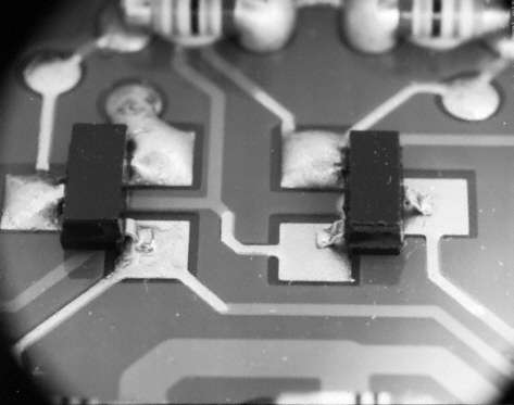
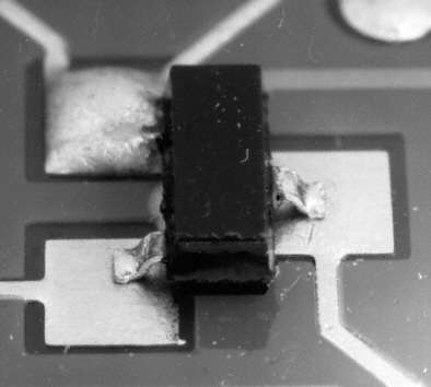
Description:
Several opens at SOT23 components after wave soldering. The leads show residues of solder in contact with which they were during the soldering process. But there are no traces of solder on the landing pads. This indicates that soldering could not take place due to poor wettability of the landing pads
Causes/Remedy:
- non-wettability of the contact configuration (pad)
- shadowing effect (layout)
- contamination of surfaces to be soldered
- corrosion of surfaces to be soldered
 Source:
visual, optical inspection - general view
 Source:
visual, optical inspection - general view
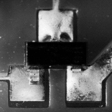
Description:
Open at a SOT23.
Causes/Remedy:
- non-wettability of the contact configuration (pad)
- shadowing effect (layout)
- contamination of surfaces to be soldered
- corrosion of surfaces to be soldered
 Source:
visual, optical inspection - general view
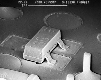
Description:
Open and lean solder fillets at a SOT 23 after wave soldering. The pads show only slight wetting or no wetting at all.
Causes/Remedy:
- non-wettability of the contact configuration (pad)
- shadowing effect (layout)
- contamination of surfaces to be soldered
- corrosion of surfaces to be soldered
 Source:
SEM
Opens at passives
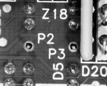
Description:
Open at a through-hole component (seen from the underside). The wave soldering process did not produce solder joints for either of the contacts nor did the solder fill the through-holes. This defect can be easily located, since it is optically very different from soldered joints.
Observe precautions for handling ESD!
Causes/Remedy:
- wetting deficiencies at leads
- wetting deficiencies at through-hole
- through-hole plating faulty/missing
- shadow effect during wave soldering
 Source:
SEM
Description:
Open at a THD (resistor, second from right). It is evident that solder is missing in the TH with the pin. The adjacent solder joints show a reduced solder filling, which is still acceptable according to IEC 61191.
Causes/Remedy:
- poor wettability of the pins
- residues/contamination in the through-hole
- poor metallic structure in the through-hole (tinning)
- unsuitable layout for the wave soldering direction
 Source:
visual, optical inspection - general view
Opens at TO220
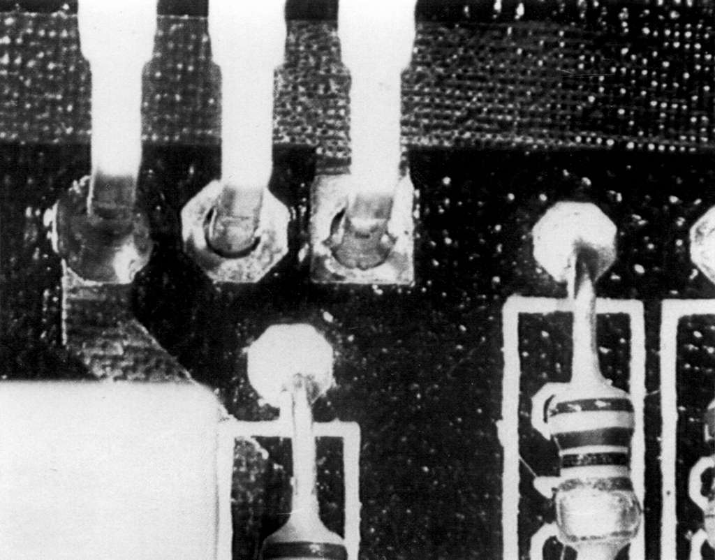
Description:
Open at a TO220. (middle, right) It is clearly visible that the solder fillet is missing at two of the pins. Optical control is often difficult, because the component body is in the way. Repair has to make sure that the solder completely fills the through-hole. Pay attention to solder contact time and soldering temperature (≤ 360 °C).
Observe precautions for handling ESD!
Causes/Remedy:
- wetting deficiencies at leads
- solder contact time during wave soldering too short
- shadow effect during wave soldering
- damaged through-hole
- soldering temperature insufficient
- flux does not reach relevant area
 Source:
visual, optical inspection - general view
Opens at other components
Description:
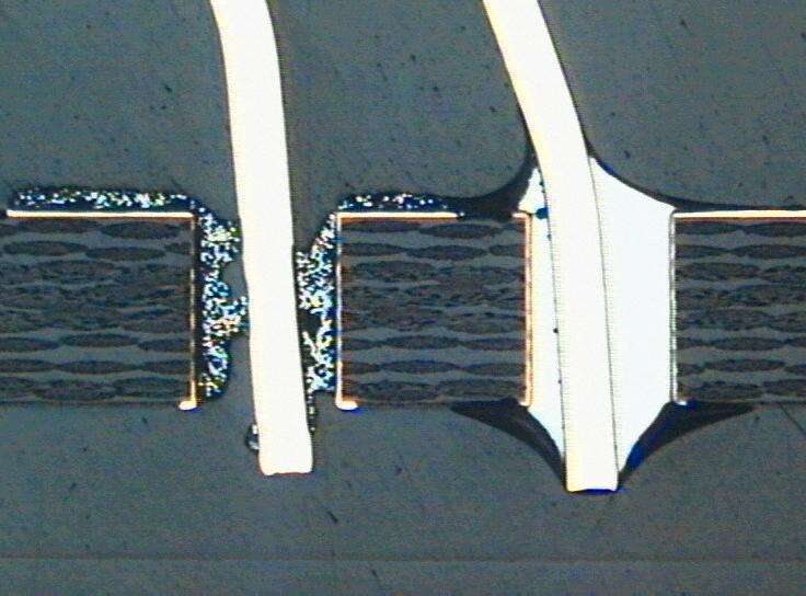
Open at a through-hole during reflow soldering. In this case an increased amount of solder paste was printed on enlarged solder eyes. The solder paste normally withdraws into the through-hole during reflow and thus connects the component with the assembly. On the photo bad heat management prevented the solder joint to form(left).It is clearly visible that the solder paste on the solder eyes and in the through-hole has not completely molten. Easily detectable defect from outside.
Causes/Remedy:
- insufficient solder paste application
- solder paste does not withdraw into through-hole
- too little heat input
- wetting deficiencies at leads
- wetting deficiencies at plated through-hole
 Source:
Microsection
Description:
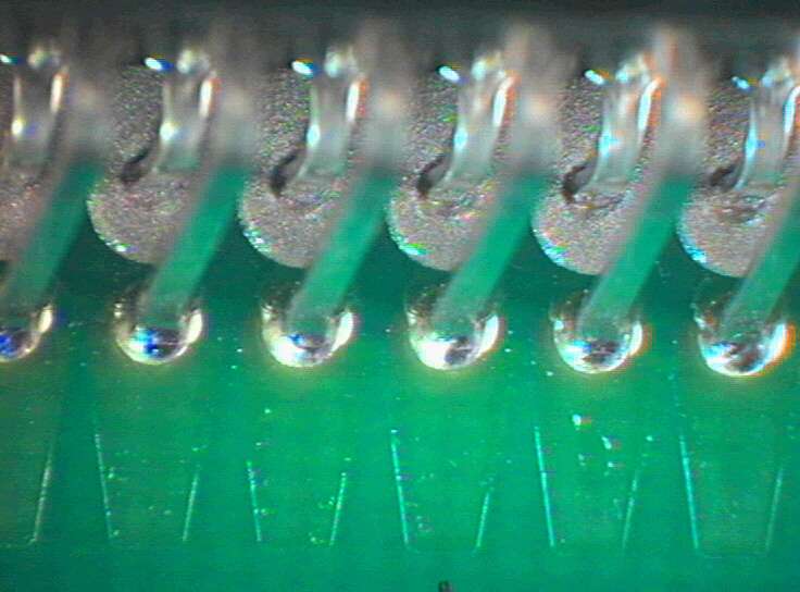
Opens at a row of plugs after through-hole reflow soldering process.
Causes/Remedy:
- too little solder paste applied
- solder paste does not enter through-holes
- too little heat energy applied
- poor wetting at the contacts
- poor wetting at the through-holes
 Source:
visual, optical inspection - general view
Our analytics team can help you find the cause.
go to failure analysis at TechnoLab
