Oblong excess solder with pointed tip, mainly to be detected at solder joints.
Solder icicle, general
Description:
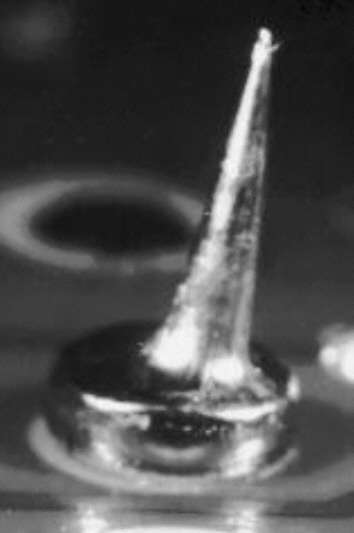
Solder icicle at a screw. Solder icicles mainly form at poorly wettable parts the wettability of which is impaired through their material properties or dewetting. But unsuitable soldering parameter (soldering temperature too low, soldering time too short) can also be responsible for this defect.
Causes/Remedy:
- poor wettability of component/PCB
- unsuitable soldering parameter: soldering temperature too low, soldering time too short
 Source:
visual, optical inspection - general view
Solder icicle at CMC
Description:
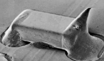
Solder icicle at a CMC1206. Formation of icicle due to beginning dewetting of contact metallization of component. Too low a soldering temperature and too short a soldering time can also be responsible for it. This defect is partly tolerable. But rework is recommended in any case.
Causes/Remedy:
- poor wettability of component/PCB
- unsuitable soldering parameter: soldering temperature too low, soldering time too short
- too little/no flux application
 Source:
SEM
Solder icicle at MiniMELF
Description:
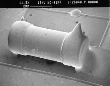
Solder icicle at a MiniMELF. In this case there is no dewetting (homogenous and wetted metallization); unsuitable soldering parameter are responsible. This defect is partly tolerable.
Causes/Remedy:
- poor wettability of component/PCB
- unsuitable soldering parameter: soldering temperature too low, soldering time too short
- too little/no flux application
 Source:
SEM
Solder icicle at THD
Description:
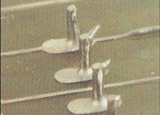
Solder icicles at the pin ends of THDs. This defect can also happen with the right soldering temperature and soldering time if the other soldering parameter are unsuitable. Excess solder which is the result of a wrongly set soldering angle and/or push-up can also lead to this effect. Partly tolerable defect.
Causes/Remedy:
- poor wettability of component/PCB
- unsuitable soldering parameter: soldering temperature too low, soldering time too short
- too little/no flux application
 Source:
visual, optical inspection - general view
Solder icicle on packages
Description:
Solder icicle at an IC package. Solder residue has adhered to the non-wettable material (plastics). This is coincidental and due to the surface structure of the package and the soldering parameter fixed. Such solder residues have to be removed, because they can get loose and cause electrical defects (short-circuits).
Causes/Remedy:
- unsuitable soldering parameter
- unsuitable surface of component
 Source:
visual, optical inspection - general view
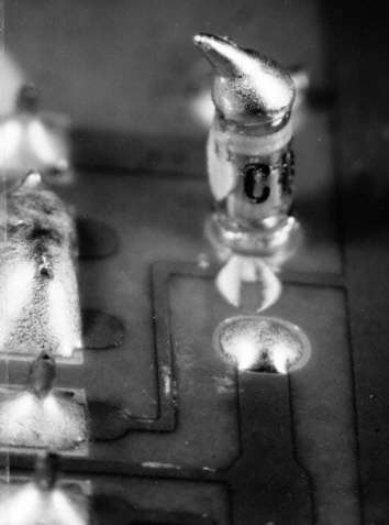
Solder icicle at SOD
Description:
Soldering icicle at a SOD which has come off its normal position. The cause is not to be found with the typical defects in this case. During wave soldering the component has come off, and solder has accumulated at the well wetted metallization to form the icicle. Though the photo shows an icicle this is only a minor fault. Rework is necessary. The component should be replaced.
Causes/Remedy:
- adhesive not hardened
- contaminated surface of component/PCB
 Source:
visual, optical inspection - general view
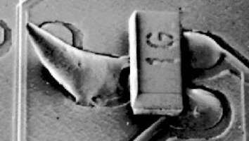
Solder icicle at SOT23
Description:
Solder icicle at a SOT23. The icicle and two other "fat" solder joints are distinctly visible. This appearance clearly indicates unsuitably set soldering parameter. Rework is necessary, because the icicle is in the vicinity of a conductor. The unshiny surface indicates that the soldering temperature was too low.
Causes/Remedy:
- poor wettability of component/PCB
- unsuitable soldering parameter: soldering temperature too low, soldering time too short
- too little/no flux application
 Source:
SEM
Our analytics team can help you find the cause.
go to failure analysis at TechnoLab
