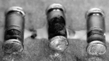
Dewetting and/or deposition of solder has taken place, but layer thickness is inhomogenous.
Description:
Dewetting of the contact areas of SOD after wetting test on arrival. First the solder wets the whole contact area, but afterwards it withdraws and leaves partial solder heaps. Such components later negatively influence solder quality.
Causes/Remedy:
- Polllution of basic metallization
- Separation of basic metallization
- unsuitable soldering parameter (temperature)
 Source:
visual, optical inspection - general view
Description:
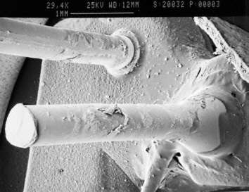
Dewetting at pins of components for through-hole mounting. Direct negative effects on the solder quality/solder joint quality can be expected. The components should not be used.
Causes/Remedy:
- Polllution of basic metallization
- Separation of basic metallization
- unsuitable soldering parameter (temperature)
 Source:
SEM
Description:
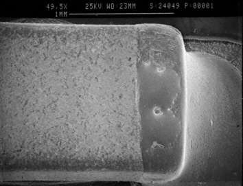
Dewetting on the upper contact area of a CMC after wave soldering. The areas where the solder has withdrawn are clearly visible. This case is debatable, since the solder joint is otherwise acceptable.
Causes/Remedy:
- Polllution of basic metallization
- Separation of basic metallization
- unsuitable soldering parameter (temperature)
 Source:
SEM
Description:
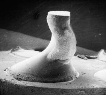
Dewetting of a pin for through-hole assembly. The area where the solder has withdrawn is clearly visible. The surface of the pin has presumably changed due to bending, so that wetting properties have changed as well.
Causes/Remedy:
- Polllution of basic metallization
- Leaching of the base metallizations
- unsuitable soldering parameter (temperature)
 Source:
SEM
Our analytics team can help you find the cause.
go to failure analysis at TechnoLab