Ball-like solder residues / blobs (diameter between rarely >0.2mm and frequently <0.05mm), partly statistically distributed, partly clustered around solder joints.
Microballs under BGAs
Description:
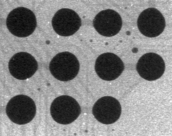
Microballs under a BGA. Many small microballs can be seen between the solder joints of the BGA. Visual control is hardly feasible without costly apparatuses, because the solder joints are hidden under the component. Loose microballs can cause electric short-circuits. Rework (cleaning) is necessary. In this case, however, this is hardly possible. (Process optimization).
Causes/Remedy:
- displacement during printing of solder paste
- smeared solder paste
- dirty stencil
- solder paste has absorbed water (hydrophilic)
- heat increase too fast during soldering
- solderability deficiencies of pads and pins
- poor contour stability of solder paste
- oxyde content of solder powder too high
- flux activitation too weak
 Source:
X-Ray
Microballs at CMCs
Description:
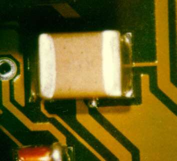
Microball at a CMC 0805. The example shows a typical connected solder ball which is very common with passive components. After placing, a capillary gap forms under the component which can suck in flux and solder particles of the solder paste The adhesion, cohesion and gravitational forces prevailing during soldering make this gap shrink considerably. The solder is squeezed out from under the component and forms a microball due to its surface tension.
Causes/Remedy:
- faulty solder paste printing
- unsuitable or wrong dimensions of landing pads
- wetting problems during the melting process
- smeared solder paste
- dirty printing stencil
 Source:
visual, optical inspection - general view
Description:
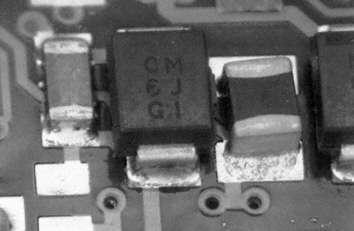
Microball by the side of the left CMC (connected solder ball).
Causes/Remedy:
- faulty solder paste printing
- unsuitable or wrong dimensions of landing pads
- wetting problems during the melting process
- smeared solder paste
- dirty printing stencil
 Source:
visual, optical inspection - general view
Description:
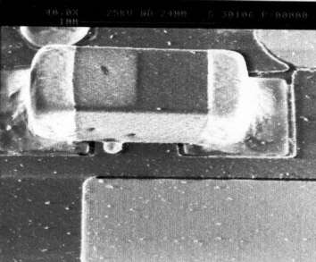
Microball by the side of the CMC (connected solder ball)
Causes/Remedy:
- faulty solder paste printing
- unsuitable or wrong dimensions of landing pads
- wetting problems during the melting process
- smeared solder paste
- dirty printing stencil
 Source:
SEM
Description:
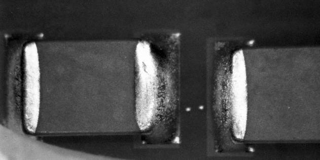
Microballs between two CMC components. If the microballs come off easily, the assembly should be cleaned.
Causes/Remedy:
- faulty solder paste printing
- unsuitable or wrong dimensions of landing pads
- wetting problems during the melting process
- smeared solder paste
- dirty printing stencil
 Source:
visual, optical inspection - general view
Microballs, general
Description:
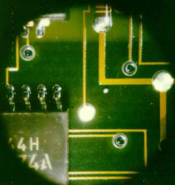
Single microball after reflow soldering. Pay attention as to whether this phenomenon is systematic or not. In our example it is not a systematic fault. The microball has formed due to smeared solder paste during the soldering process. Cleaning is to be done if the single microballs easily come off the assembly.
Causes/Remedy:
- displacement during printing of solder paste
- smeared solder paste
- dirty printing stencil
 Source:
visual, optical inspection - general view
Microballs at SO
Description:
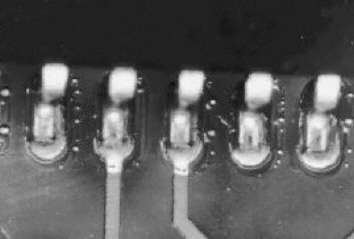
Microballs between the leads of a SO-IC. Badly wetted or unwetted PCB surfaces can lead to the formation of microballs due to the solder repelling from the unwetted surface. Cleaning is absolutely necessary, because loose microballs can cause short- circuits.
Causes/Remedy:
- flux activitation too weak
- oxyde content of solder powder too high
- poor contour stability after printing
- solderability deficiencies of pads and pins
- poor reflow profile
 Source:
visual, optical inspection - general view
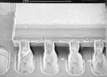
Description:
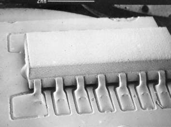
Single microballs between the solder joints of a SO16 after wave soldering. It is recommended to remove the microballs from the assembly if this can be easily done. It should be tested which solder stop masks especially favour the formation of microballs.
Causes/Remedy:
- poor flux application
- flux not active enough
- unsuitable solder stop (surface)
- unsuitable soldering process parameter
 Source:
SEM
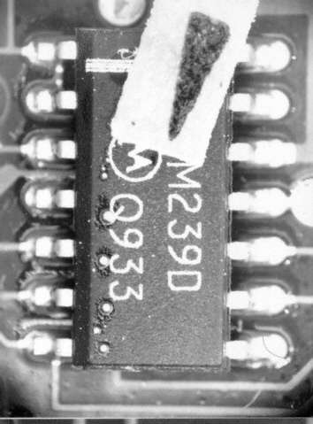
Description:
Microballs on the casing surface of a SO14 after wave soldering. This easily detectable defect is very rare. It can be caused by unsuitable process parameter (soldering angle, soldering temperature, etc.) and a coarse surface of the IC.
Causes/Remedy:
- unsuitable soldering parameter (soldering angle, temperature)
- significant rise in the coarseness of the surface of the IC casing
- Flux process favours formation of microballs
 Source:
visual, optical inspection - general view
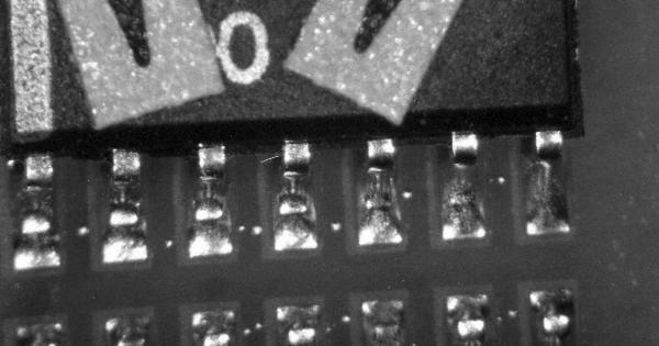
Description:
Further example of microballs between the solder joints of a SO-IC after wave soldering.
Causes/Remedy:
- poor flux application
- flux not active enough
- unsuitable solder stop (surface)
- unsuitable soldering process parameter
 Source:
SEM
 Source:
visual, optical inspection - general view
Microballs at SOT23
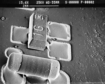
Description:
Single microball at a SOT 23 after wave soldering. The solder resist mask ( surface condition, topology, temperature reaction) is the main factor which influences this phenomenon.
Causes/Remedy:
- deficiencies in flux application
- flux activitation too weak
- poor solder resist (surface)
- poor soldering process parameter
 Source:
SEM
Microballs at passives
Description:
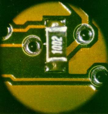
Microball at a chip resistor, same characteristic as described for CMC
Causes/Remedy:
- faulty solder paste application
- unsuitable or wrong dimensions of landing pads
- wetting problems during the melting process
- smeared solder paste
- dirty printing stencil
 Source:
visual, optical inspection - general view
Our analytics team can help you find the cause.
go to failure analysis at TechnoLab
