Solder between electrical contacts which must be insulated from each other.
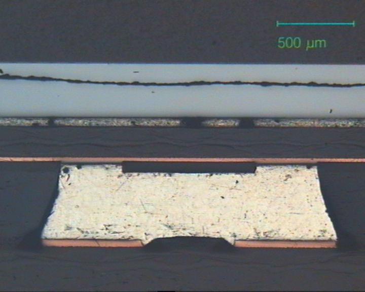
Solder bridge under BGA
Beschreibung:
Solder bridge under a PBGA caused by interfusion of two solder depots during the reflow soldering process. This defect is not or only hardly visible from outside, because the solder joints are under the component. In general, only X-ray inspection can detect such defects. This defect can only be repaired by completely removing the component and subsequently place it back so that good rework knowledge is essential.
Causes/Remedy:
- excessive solder paste
- movement of component during reflow
- torsion of component due to popcorning
- inexpert execution/position of the plated through holes
- missing or damaged solder resist mask
- smeared solder paste
 Source:
Microsection
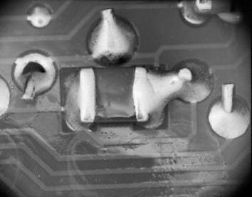
Solder bridge at CMC
Description:
Solder bridge at a CMC during wave soldering. Easily discernible defect. The solder bridge is between the SMC component and the pin of a THD. Rework is easy. Observe suitable solder parameter. Solder tip temperature
Causes/Remedy:
- wrong soldering direction / layout
- faulty layout / minimum distances
- pollution of solder
- poor soldering parameter: soldering angle, push-up, flux
 Source:
visual, optical inspection - general view
Description:
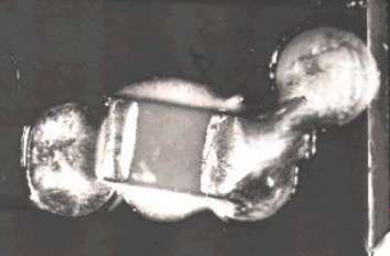
Solder bridge at a CMC. The solder has formed a bridge to the neighbouring, wettable area during the wave soldering process. Moreover the component is misaligned, which is probably due to adhesive not completely hardened. The component was shifted during soldering so that the minimum distance between adjacent wettable areas was not kept.
Moreover the adhesive reaches the componend landing pads
Causes/Remedy:
- adhesive not completely hardened
- unsuitable type of adhesive
- too much adhesive
- contaminated surface of component / adhesive force/wetting insufficient
 Source:
visual, optical inspection - general view
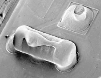
Solder bridge at MiniMELF
Description:
Solder bridge over a MiniMELF resistor. The photo shows a rather rare and unusual soldering defect. It is easily detectable because the (reflecting) solder is well discernible. We recommend to completely remove the component from the assembly in order not to touch the delicate ceramic body with a soldering iron.
Causes/Remedy:
- formation of dross in the solder
- poor soldering parameter: soldering angle, push-up
- pollution of solder (alloy)
 Source:
SEM
Solder bridges at QFP
Description:
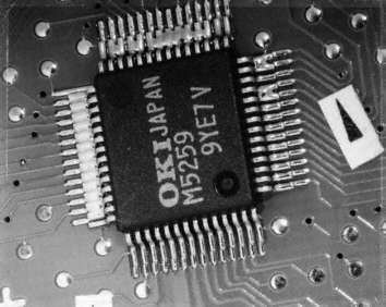
Solder bridges at a QFP 56 after wave soldering. In addition to soldering this example also shows heavy disalignment of the component in comparison to its ideal position. The latter fact only slightly contributes to the formation of solder bridges though. During rework the component has to be removed, placed back and duly soldered.
Observe precautions for handling ESD!
Causes/Remedy:
- formation of dross in the solder
- poor soldering parameter: soldering angle, push-up
- pollution of solder (alloy)
- wrong soldering direction
- absence of solder thieves
 Source:
visual, optical inspection - general view
Description:
Numerous solder bridges at the leads of a QFP.
Causes/Remedy:
- formation of dross in the solder
- unsuitable soldering parameter: soldering angle, push-up, temperature
- contamination of the solder (alloy)
- unsuitable soldering direction
- non-existance of solder thieves
 Source:
visual, optical inspection - general view
Solder bridges at SO
Description:
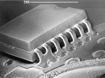
Solder bridge at a SO14 after wave soldering. This soldering defect is incidental. It is easily located by well-trained inspection staff.
Observe precautions for handling ESD!
Causes/Remedy:
- poor soldering parameter: soldering angle, push-up
- wrong soldering direction
- absence of solder thieves
 Source:
SEM
Description:
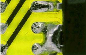
Solder bridge at a SO-IC after wave soldering. This soldering defect is clearly discernible, since the gullwings are to the outside and thus easily inspectable
Causes/Remedy:
- unsuitable soldering parameter: soldering angle, push-up, temperature, advance speed
- unsuitable soldering direction
- non-existance of solder thieves
 Source:
visual, optical inspection - general view
Description:
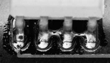
Solder bridges at a SO8 component. Example of bridge causing further bridges Folgebrücken.
Causes/Remedy:
- unsuitable soldering parameter: soldering angle, push-up, temperature, advance speed
- unsuitable soldering direction
- non-existance of solder thieves
 Source:
visual, optical inspection - general view
Description:
Single solder bridge at a SO14. The rare single solder bridge can be classified as coincidental, if otherwise the soldering parameter show satisfactory results.
Causes/Remedy:
- unsuitable soldering parameter: soldering angle, push-up, temperature, advance speed
- unsuitable soldering direction
- non-existance of solder thieves
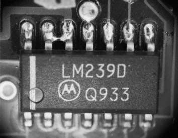 Source:
visual, optical inspection - general view
Description:
Solder bridge between a lead and the solder thief. (which is the outer pad and is only there to separate or tear off the solder from the last lead, depending on the soldering direction). This solder bridge has only optical importance, since the electrical function is given. No rework necessary, if not required otherwise.
Causes/Remedy:
- unsuitable soldering parameter: soldering angle, push-up, temperature, advance speed
- unsuitable soldering direction
- non-existance of solder thieves
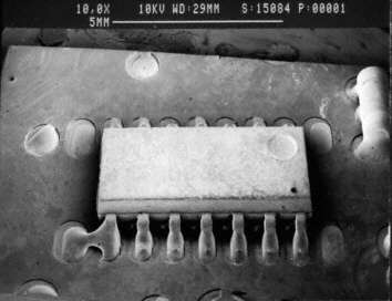 Source:
SEM
Solder bridge at SOT23
Description:
Solder bridge at a SOT23 capacitor between landing pad and the adjacent check point. What is striking here is that the solder joint below does not have enough solder by far. It is likely that solder has drained from this site during soldering and was deposited at the top solder joint instead where it has formed a solder bridge.
Observe precautions for handling ESD!
Causes/Remedy:
- wrong soldering direction
- faulty layout / minimum distances
- faulty solder resist
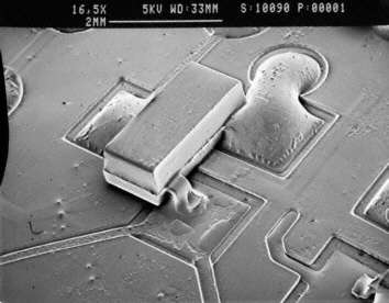 Source:
SEM
Description:
Solder bridge between the two contact leads of a SOT23. It can be seen that after the wave soldering process solder is sticking to the component body. This defect is quite rare, but it illustrates the great variety of possible defects. This solder bridge was caused by unsuitable soldering parameter and/or contaminated solder.
Causes/Remedy:
- contamination of solder
- dross abets formation of solder bridges/solder flags
- unsuitable soldering parameter
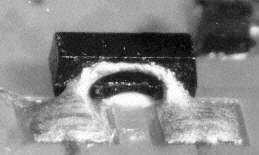 Source:
visual, optical inspection - general view
Solder bridge at SOT89
Description:
Solder bridge between two leads of a SOT89. No systematic defect, but due to deviations from the processing parameter or defects on the assembly. This defect can easily be repaired by removing the solder bridge.
Observe precautions for handling ESD!
Causes/Remedy:
- wrong soldering direction
- poor soldering parameter: soldering angle, push-up
- pollution of the solder (alloy)
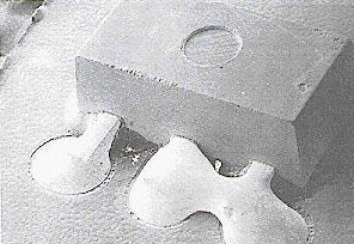 Source:
visual, optical inspection - general view
Solder bridge at LCCC
Description:
Solder bridge at a LCCC after wave soldering. We recommend to completely remove the solder of the two solder joints concerned and then produce solder joints using suitable soldering parameter. Solder tip temperature Observe precautions for handling ESD!
Causes/Remedy:
- wrong soldering direction
- poor soldering parameter: soldering angle, push-up
- faulty layout / minimum distances
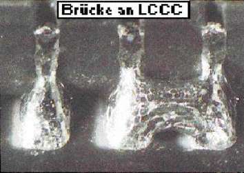 Source:
visual, optical inspection - general view
Solder bridge at SOD
Description:
Solder bridge between two adjacent SOD components after wave soldering. Displacement can lead to too close placing of components so that minimum distances are not adhered to. During rewok both solder joints should be completely cleared of solder, afterwards suitable soldering parameter should be used for soldering. Solder tip temperature Observe precautions for handling ESD!
Causes/Remedy:
- wrong soldering direction
- poor soldering parameter: soldering angle, push-up
- faulty layout / minimum distances
- minimum distance not adhered to
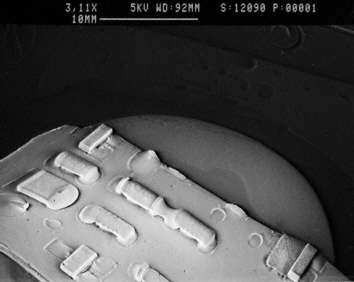 Source:
SEM
Solder bridge at other components
Description:
Solder bridge at a socket bank after wave soldering. Easily detectable defect. Rework must make sure that the contacts are not damaged and that sufficient solder is deposited in the through-hole.
Causes/Remedy:
- wrong soldering direction
- poor soldering parameter: soldering angle, push-up
- pollution of solder (alloy)
- disturbed flux application
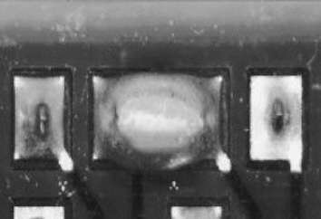 Source:
visual, optical inspection - general view
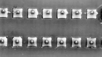
Description:
Clearly visible beginning of solder bridges in the top row on the left . Following the soldering direction a solder thread has formed towards the adjacent soldering joint. The risk of bridges is very high.
Causes/Remedy:
- Soldering direction abets formation of bridges. The row of soldering joints is the same as the soldering direction!
- unsuitable soldering parameter
- formation of dross/polluted solder
 Source:
visual, optical inspection - general view
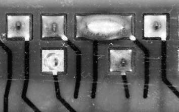
Description:
Solder bridge between two neighbouring contacts. This defect indicates an unsuitable soldering direction, but it can also happen for other reasons, even with the best soldering direction.
Causes/Remedy:
- Soldering direction abets formation of bridges. The row of soldering joints is the same as the soldering direction!
- unsuitable soldering parameter
- formation of dross/polluted solder
 Source:
visual, optical inspection - general view
Our analytics team can help you find the cause.
go to failure analysis at TechnoLab
