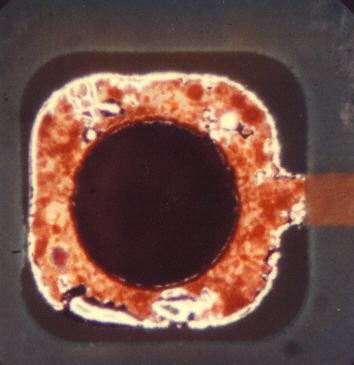
Contamination / corrosion
Description:
Contamination and corrosion on the copper surface caused by problems tinning this eyelet. Moreover there are areas on the copper where the base material is shining through (light areas) because the copper layer is too thin. Not acceptable because soldering can become impossible.
Causes/Remedy:
- galvanizing fault of manufacturer
 Source:
visual, optical inspection - general view
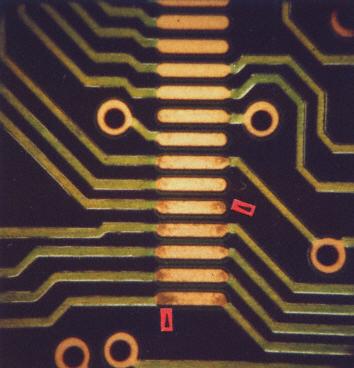
Faulty gold plating
Description:
Faulty galvanizing process. During electro-plating too few gold was separated at the areas marked. The layer underneath (Ni) shows first traces of corrosion. Not acceptable, since it can lead to defects during soldering.
Causes/Remedy:
- poor electro-plating process
- insufficient preparation of board (cleaning, layers underneath)
 Source:
visual, optical inspection - general view
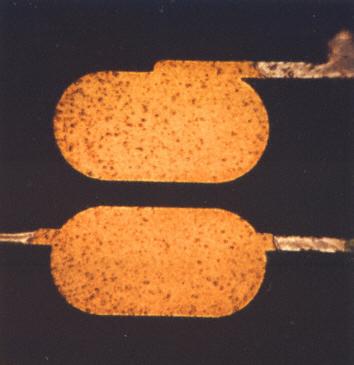
Formation of knots
Description:
Formation of knots on the Ni barrier under the covering gold layer.An unfavorable current distribution during the electro-plating process caused the formation of many little knots in the middle layer (see photo below, microsection) which penetrate the gold layer. The general view clearly shows the knots. This board should not be used because soldering and contact problems are likely.
Causes/Remedy:
- poor electro-plating process
- middle gold layer penetrates gold layer on top
 Source:
visual, optical inspection - general view
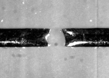
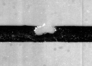
Break
Description:
Break of a conductor. A faulty galvanic process in the manufacture of the board (subtractive process) led to a part of the conductor being etched away. This defect is an indication for blank parts in the photo resist. Manufacturing fault. This board must not be used.
Causes/Remedy:
- electro-plating defect during manufacture of PCB
- faulty photo resist / fault in the manufacturing process
 Source:
visual, optical inspection - general view
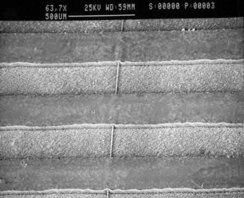
Partial break
Description:
Same context as described before, but in this case the conductor has not completely broken. Electrical function is there, but problems can arise under electrical load. This board must not be used.
Causes/Remedy:
- electro-plating defect during manufacture of PCB
- faulty photo resist / fault in the manufacturing process
 Source:
visual, optical inspection - general view
Inclusion
Description:
Foreign inclusion in conductors. It is probably a glass fibre from the base material. As this foreign inclusion reduces the thickness of the conductors, this defect is not acceptable
Causes/Remedy:
- defect in the manufacture of the base material
 Source:
SEM
Our analytics team can help you find the cause.
go to failure analysis at TechnoLab