Solder fillet by far above specification limit.
Attention ! Always compare with current specifications and standards. They often differ from each other. Here DIN EN 61191, Part 1 - 4, and IEC 61191, Part 1 - 4 respectively are taken as reference basis. The assessment of all solder joints is based on the standards given above.
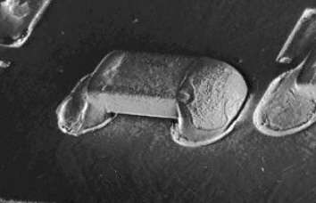
Excessive solder at CMC
Description:
Borderline case of excessive solder at a CMC after wave soldering. The relatively fat solder joint is just acceptable. The solder may reach over the contact area or up to the top edge of the contact metallization, but it must not reach over the body of the component.
Causes/Remedy:
- poor layout design
- pollution of the solder (alloy)
- poor process parameter (wave soldering)
 Source:
SEM
Description:
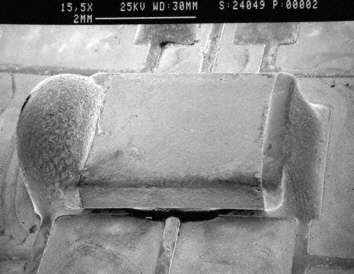
Excessive solder on one side of a CMC. In accordance with IEC 61191 this solder joint has to be reworked. Solder joints such as this often cause rapid failure or possess bad mechanical properties.
Causes/Remedy:
- unsuitable soldering parameter (temperature, soldering angle, etc.)
- unsuitable soldering direction
- wetting problems at the component/landing pads
 Source:
SEM
Description:
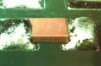
Excessive solder at both ends caused by landing pads unsuited for this type of component. As a consequence the solder joints have adopted a nonconforming shape.
Causes/Remedy:
- Layout / landing pads of component wrong/unsuited
 Source:
visual, optical inspection - general view
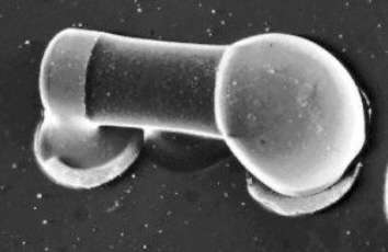
Excessive solder at MiniMELF
Description:
Excessive solder at a MiniMELF resistor after wave soldering.The solder reaches beyond the contact metallization and touches the component body.The solder joint has to be reworked in any case. (observe soldering temperature, T ≤ 350°C)
Causes/Remedy:
- poor layout design
- pollution of the solder (alloy)
- poor process parameter (wave soldering)
 Source:
SEM
Description:
Excessive solder on one side of a MiniMelf after wave soldering.The shape of the soldering joint is still acceptable according to the standards, but the solder touches the component body. Therefore the fault is non-conforming. Rework is necessary.
Causes/Remedy:
- poor soldering parameter (temperature, soldering angle, etc.)
- unsuitable soldering direction
- wetting problems at the component/landing pads
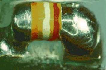 Source:
visual, optical inspection - general view
Description:
Same defect as described above. Rework necessary.
Causes/Remedy:
- poor soldering parameter (temperature, soldering angle, etc.)
- unsuitable soldering direction
- wetting problems at the component/landing pads
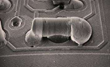 Source:
SEM
Excessive solder at PLCC
Description:
Borderline case of excessive solder at a PLCC. It is clearly visible that the solder has crept up the leads. As long as the solder does not come into contact with the component body, the solder joints are acceptable. It has to made sure, however, that there is a solder fillet at the toe as well as at the heel of the lead.
Causes/Remedy:
-/-
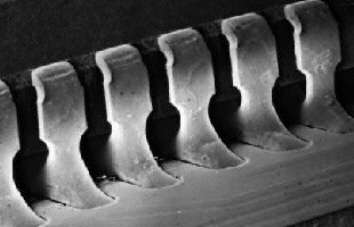 Source:
SEM
Excessive solder at SO
Description:
Excessive solder at two gullwing-leads of a SO component. During repair solder in excess quantity was deposited at the leads. According to IEC 61191 - 2 these two solder joints are still acceptable.As the width of the solder joints exceeds that of the leads, it cannot be ruled out that the minimum distance between two neighbouring conductors is not adhered to. Make sure that there are solder fillets at the heels ot the leads.
Causes/Remedy:
- repair soldering: solder fillet too big
- inexpert carrying-out of rework
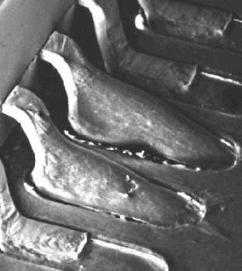 Source:
SEM
Description:
General view of the example shown above
Causes/Remedy:
- repair soldering: solder fillet too large
- inexpert repair work
 Source:
SEM
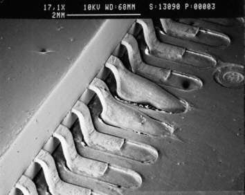
Description:
Rich solder joint at a L-lead. This solder joint is a borderline case for excessive solder. Since the solder does not touch the component body, the soldering result is still acceptable according to IEC 61191-2.It has to be made sure that wetting and solder fillet are immaculate.
Causes/Remedy:
- poor process parameter for wave soldering(soldering angle, temperature)
- contamination of the solder/alloy
- poor flux / flux application
 Source:
visual, optical inspection - general view
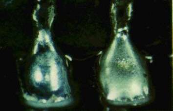
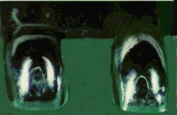
Description:
Same context as described above.
Causes/Remedy:
- poor process parameter for wave soldering (soldering angle, temperature)
- contamination of the solder/alloy
- poor flux / flux application
 Source:
visual, optical inspection - general view
Excessive solder at SOT23
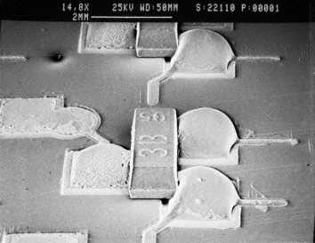
Description:
Excessive solder at SOT23 components after wave soldering. The photo shows that the solder touches the component body. According to IEC 61191-2 the solder joints are not acceptable and have to be reworked.
Observe precautions for handling ESD!
Causes/Remedy:
- poor process parameter during wave soldering (soldering angle, temperature)
- pollution of the solder /alloy
- poor flux/flux application
 Source:
SEM
Description:
Borderline case of excessive solder. The solder joint is acceptable, since the solder does not touch the component body. Nevertheless it would be wise to find out whether this was caused by a systematic fault.
Causes/Remedy:
- Poor process parameter
- unsuitable flux / poor flux application
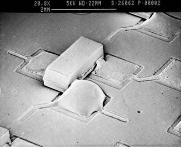 Source:
SEM
Excessive solder, general
Description:
Fat solder joint, with a wetting angle of >90°. According to EC 61191-1 this is a borderline case which is acceptable, however. It should be made sure nevertheless that the majority of solder joints has a wetting angle of < 90° and is concave to the lead of the component respectively.
Causes/Remedy:
- poor process parameter during wave soldering (soldering angle, temperature)
- pollution of the solder /alloy
- poor flux/flux application
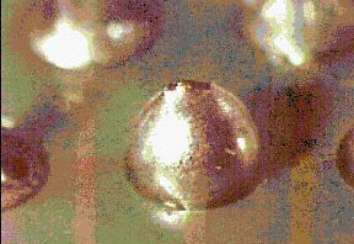 Source:
visual, optical inspection - general view
Description:
Solder accumulated at a wettable test point on the PCB. The solder accumulation has to be removed by suitable means because it impairs the subsequent electrical test.
Causes/Remedy:
- poor parameter of the wave soldering process (soldering angle, temperature)
- contamination of the solder / alloy
- unsuitable flux / poor flux application
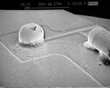 Source:
SEM
Our analytics team can help you find the cause.
go to failure analysis at TechnoLab
