Uneven surface
Description:
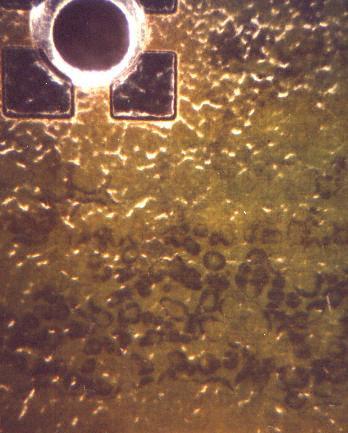
Uneven surface (rough, orange skin effect) due to partial separation of solder resist from PCB. This phenomenon is especially frequent in areas under which there are tinned conductors and copper. With the separation the resist often develops cracks which allow humidity to affect the conductors. The resulting corrosion reduces the insulating capacity.
Causes/Remedy:
- unsuitable solder resist
- contamination of parts of PCB
- insufficient heat resistance of finish
 Source:
visual, optical inspection - general view
Displacement of resist
Description:
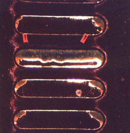
Displacement of resist from its ideal position. This very frequent defect has considerable influence on the quality of the solder joints, since the wettable areas (as shown in the photos) can be reduced decisively and/or covered totally. Not acceptable.
Causes/Remedy:
- poor finish application process
- poor stripping of the resist
- faulty layout (light exposure)
 Source:
visual, optical inspection - general view
Description:
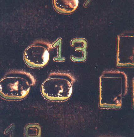
Displacement of resist from its ideal position
Causes/Remedy:
- poor finish application process
- poor stripping of the resist
- faulty layout (light exposure)
 Source:
visual, optical inspection - general view
Inclusions
Description:
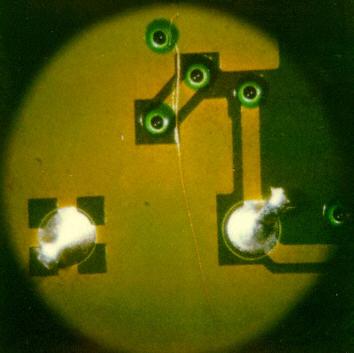
Inclusion of undefined particles under the finish. This manufacturing error can lead to short circuits (conductive inclusions). These PCBs must not be used.
Causes/Remedy:
- manufacturing defect
- contamination of uncoated base material
 Source:
visual, optical inspection - general view
Missing resist
Description:
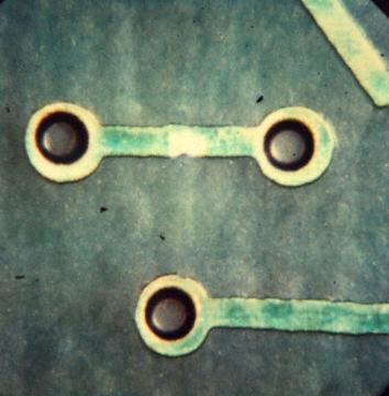
Resist partially non-existent and unevenly thick. This defect only appears in the pouring process of liquid resist application. The inhomogenous distribution of the resist can also lead to spots where the resist is totally non-existent. Conductors which have not been covered can cause corrosion which in its turn can influence the electric properties of the assembly.
Causes/Remedy:
- poor resist application process
- unsuitable resist
- surface of base material uneven, bad distribution of resist
 Source:
visual, optical inspection - general view
Description:
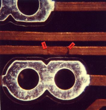
Resist lacking directly on a conductor. There is the risk of bridging between the eyelet and the wettable conductor area during the soldering process. In most of the cases this phenomenon is caused by contamination of the board areas underneath. Rework is necessary.
Causes/Remedy:
- Contamination (fat) of the PCB
- faulty resist application leaving uncovered areas
- mechanical damage to resist (resist peeling off)
 Source:
visual, optical inspection - general view
Cracks
Description:
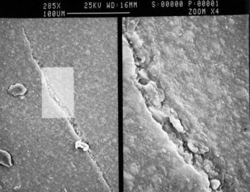
Cracks (microcracks) in the surface of the solder resist. Faulty processing (tension, bending of base material) causes cracks in the resist. . Humidity penetrating into the material can later cause corrosion on the conductive areas. Corrosion is especially problematic with conductors, because electromigration has a strong negative influence on the insulating strength.
Causes/Remedy:
- poor solder resist
- mechanical stress causes resist to crack
- faulty processing of resist
 Source:
SEM
Description:
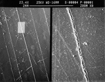
same context as described above, but in this case the cracks were caused mechanically, e.g. during transport.
Causes/Remedy:
- inexpert handling of the board/assembly
- solder resist too weak as far as mechanical stress is concerned
 Source:
SEM
Peeling, wrinkling
Description:
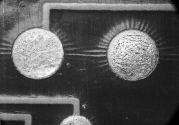
Peeling-off at, wrinkling around two through-holes fillet with solder. Thermal stress during soldering in combination with a poor layout (resist is too close to the through-holes) caused the defects shown in the photo.
Causes/Remedy:
- poor thermal properties of the resist
- unsuitable soldering process parameter (temperature)
- faulty layout for application of resist
 Source:
visual, optical inspection - general view
Our analytics team can help you find the cause.
go to failure analysis at TechnoLab
